- Description
- Specifications
- Videos
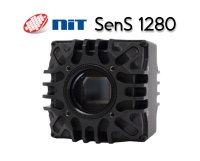
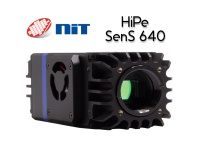
NIT, the world leaders of SWIR cameras, brings you the SenS 1280 Smart SWIR camera. This compact and affordable Smart SWIR camera is for high-definition imaging applications were resolution matters. The SXVGA (1280 X 1024) format with 10 um pixel size along with a very low noise floor (< 30e-) makes a very dynamic Smart SWIR camera.
NIT has developed and invested into a manufacturing line making state-of-the-art InGaAs sensors using a unique and proprietary technology capable of ensuring the stacking of the InGaAs array with the CMOS read out circuit at a sub-micron precision with extremely high yield.
Equipped with advanced onboard image processing, the SenS 1280 HD SWIR camera-Smart version guarantees unparalleled performance. Here’s what it offers:
- Automatic Gain Control (AGC): Ensures optimal brightness and contrast levels, enabling precise detail capture even in challenging lighting conditions. This eliminates the need for manual adjustments and simplifies the imaging process.
- Automatic Integration Time (AIT): The camera can automatically adjust the exposure time to match a target brightness eliminating the need for manual adjustments.
- On-board Non-Uniformity Correction (NUC) and Bad Pixel Replacement (BPR): Enhance image quality by correcting irregularities and replacing defective pixels.
SenS 1280 SWIR Smart Applications:
- Machine Vision
- Semiconductor inspection
- Security & Surveillance
- Defense & Security
- High Resolution Microscopy
- Laser Beam Profiling
- Airborne Cameras
| 1280 x 1024 pixels | |
|
Key Features:
|
|
| 60Hz Full Frame | |
| CamLink, HD-SDI, CoaXPress | |
| NSC1901T-SI | |
| 10μm | |
| 10 usec - 500ms | |
| TE Cooled | |
| 58 x 58 x 70mm | |
| >80% LG | |
| InGaAs | |
| ITR, CDS, ROI | |
| CTIA High Gain (52dB) CTIA Low Gain (61dB) | |
| -40 °C to + 71 °C |
Related products
What is SWIR imaging?
(SWIR) Short-wave Infrared imaging is an advanced technique, used for producing images based on radiation within the electromagnetic spectrum. Infrared radiation is located between visible light and microwaves between 0.75 µm – 1mm wavelength. Infrared is split between 5 regions: Near-Infrared (NIR), Short-Wave Infrared (SWIR), Mid-Wave Infrared (MWIR), Long-Wave Infrared (LWIR), and Far Infrared (FIR). SWIR cameras can see even at night and under hard visible conditions lie clouds, smoke, or even dust. Another major benefit of SWIR imaging that is the ability to image through glass, great for inspection of products with no destruction.
What is a InGaAs sensors?
InGaAs is an arcanum for the element composition of the material it makes (Indium, Gallium, Arsenide). NIT has developed and invested into a manufacturing line of InGaAs sensors using a unique and proprietary technology. InGaAs annoy absorbs IR light invisible to silicon and converts incident light into electrons digitized by the ROIC and the camera electronics. Adding this array to a ROIC, read-out integrated circuits, can be a challenging task in design and engineering. One of the critical steps is the 3D stacking of the photodiode array to the read-out circuit, for which NIT has developed a very innovative flip chip process ensuring the CMOS read out circuit at a sub-micron precision high yield and low cost of production.
What applications is SWIR imaging used in?
SWIR imagers are used in a large number of applications including semiconductor inspection, laser alignment and beam profiling, hot glass inspection, security and surveillance, machine vision imaging, agricultural sensing, microscopy and life science imaging. Some examples are on our infrared and thermal imaging applications page.
Export Disclaimer: Some goods on this site may be subject to US Export Regulations. Buyer agrees as one of the terms of purchase not to export such goods without having obtained and executed proper export licenses from the United States Government. Learn more.

