- Description
- Specifications
- Videos
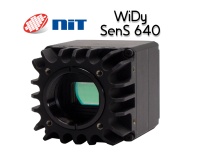
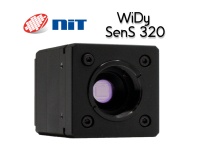
NITs cost effective solution, the HiPE SenS 640 SWIR Cameras is the best price to performance ratio on the market. With TEC2 & air-cooled operating mode, these SWIR cameras are designed for low light, long exposure time applications (from 10us to 112s). The HiPe Sens 640 can operate with an FPA temperature as low as -20°C only with internal air cooling.
NITs SWIR sensors and cameras are all manufactured in-house using unique manufacturing technologies such as small pitch high yield hybridization capacity. NIT has engineered a SWIR camera that can be easily integrated to microscope benches or any other optical devices, thanks to the small form factor.
HiPe SenS 640 applications:
- Medical & Life science
- Semiconductor inspection
- Security & Surveillance
| 640 x 512 pixels | |
|
Key Features:
|
|
| Up to 230Hz Full Frame | |
| CameraLink™ or USB 3.0 | |
| NSC1902T-SI | |
| 15μm | |
| TEC2 + Fan air-cooled | |
| Down to 16x16 | |
|
Linear, 3 gain levels |
|
| USB3.0, CameraLink | |
| >85% (90% typical) | |
| InGaAs | |
| IWR/ITR, CDS, ROI |
Related products
What is SWIR imaging?
(SWIR) Short-wave Infrared imaging is an advanced technique, used for producing images based on radiation within the electromagnetic spectrum. Infrared radiation is located between visible light and microwaves between 0.75 µm – 1mm wavelength. Infrared is split between 5 regions: Near-Infrared (NIR), Short-Wave Infrared (SWIR), Mid-Wave Infrared (MWIR), Long-Wave Infrared (LWIR), and Far Infrared (FIR). SWIR cameras can see even at night and under hard visible conditions lie clouds, smoke, or even dust. Another major benefit of SWIR imaging that is the ability to image through glass, great for inspection of products with no destruction.
What is a InGaAs sensors?
InGaAs is an arcanum for the element composition of the material it makes (Indium, Gallium, Arsenide). NIT has developed and invested into a manufacturing line of InGaAs sensors using a unique and proprietary technology. InGaAs annoy absorbs IR light invisible to silicon and converts incident light into electrons digitized by the ROIC and the camera electronics. Adding this array to a ROIC, read-out integrated circuits, can be a challenging task in design and engineering. One of the critical steps is the 3D stacking of the photodiode array to the read-out circuit, for which NIT has developed a very innovative flip chip process ensuring the CMOS read out circuit at a sub-micron precision high yield and low cost of production.
What applications is SWIR imaging used in?
SWIR imagers are used in a large number of applications including semiconductor inspection, laser alignment and beam profiling, hot glass inspection, security and surveillance, machine vision imaging, agricultural sensing, microscopy and life science imaging. Some examples are on our infrared and thermal imaging applications page.
Export Disclaimer: Some goods on this site may be subject to US Export Regulations. Buyer agrees as one of the terms of purchase not to export such goods without having obtained and executed proper export licenses from the United States Government. Learn more.

