- Description
- Specifications
- Videos
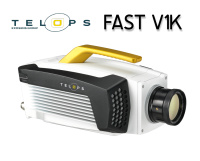
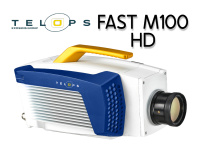
Telops introduces the FAST S1K SWIR near infrared camera
Fast S1K is Telops affordable science-grade near-infrared camera is highly sensitive from 0.9 to 1.7 µm with an InGaAs FPA. This unique SWIR camera is the fastest infrared camera reaching unrivalled low-noise levels even at an astounding 1000 frame-per-second rate at full resolution and up to 103,000 fps at 64 x 8 in subwindow mode. Either it is for fluorescent markers imaging, quality control of semiconductors, material sorting, gas detection, borehole samples analysis, solar cells characterization or space applications, the Fast S1K SWIR camera extend the boundaries of laboratory and industrial imaging. Telops FAST S1K SWIR infrared InGaAs camera is designed to provide radiometic measurements of hot targets with optional temperature calibrations between 300 to 700°C. It is easy to install on Windows platforms and presents a friendly user interface using the Reveal IR software Suite. Telops also includes MATLAB and Python integration. Its multithreaded architecture is a key feature when processing in parallel complex algorithms, acquiring, visualizing, importing and exporting data in real time. Data processing includes real-time data output, real time scene temperature calibration, real time radiance calibration, customer calibration management tools, time stamping, Telops Automatic Exposure control (AEC), enhanced high dynamic range, and a motorized filter wheel.
Target applications include:
- Detection of explosive liquid precursors
- Survailence
- Semiconductor analysis
- Environment
- Agriculture
- Solar cells characterization
| 640 x 512 pixles | |||||||||||||||||
| 16GB or 32GB | |||||||||||||||||
|
|||||||||||||||||
| up to 1000Hz full frame | |||||||||||||||||
| Gigabit Ethernet | |||||||||||||||||
| InGaAs | |||||||||||||||||
| InGaAs | |||||||||||||||||
| 20um | |||||||||||||||||
| 1 μs | |||||||||||||||||
| 13.8" X 7.8" X 6.9" | |||||||||||||||||
Telops introduces the FAST S1K SWIR near infrared camera
|
|||||||||||||||||
| Subwindow Mode | |||||||||||||||||
| GigE, Camera Link, HD-SDI | |||||||||||||||||
| InGaAs | |||||||||||||||||
| RAW, NUC, TEMP, RADIANCE | |||||||||||||||||
| GigE, Camera Link, HD-SDI | |||||||||||||||||
| -20C to +50°C |
Related products
What is SWIR imaging?
(SWIR) Short-wave Infrared imaging is an advanced technique, used for producing images based on radiation within the electromagnetic spectrum. Infrared radiation is located between visible light and microwaves between 0.75 µm – 1mm wavelength. Infrared is split between 5 regions: Near-Infrared (NIR), Short-Wave Infrared (SWIR), Mid-Wave Infrared (MWIR), Long-Wave Infrared (LWIR), and Far Infrared (FIR). SWIR cameras can see even at night and under hard visible conditions lie clouds, smoke, or even dust. Another major benefit of SWIR imaging that is the ability to image through glass, great for inspection of products with no destruction.
What is a InGaAs sensors?
InGaAs is an arcanum for the element composition of the material it makes (Indium, Gallium, Arsenide). NIT has developed and invested into a manufacturing line of InGaAs sensors using a unique and proprietary technology. InGaAs annoy absorbs IR light invisible to silicon and converts incident light into electrons digitized by the ROIC and the camera electronics. Adding this array to a ROIC, read-out integrated circuits, can be a challenging task in design and engineering. One of the critical steps is the 3D stacking of the photodiode array to the read-out circuit, for which NIT has developed a very innovative flip chip process ensuring the CMOS read out circuit at a sub-micron precision high yield and low cost of production.
What applications is SWIR imaging used in?
SWIR imagers are used in a large number of applications including semiconductor inspection, laser alignment and beam profiling, hot glass inspection, security and surveillance, machine vision imaging, agricultural sensing, microscopy and life science imaging. Some examples are on our infrared and thermal imaging applications page.
Export Disclaimer: Some goods on this site may be subject to US Export Regulations. Buyer agrees as one of the terms of purchase not to export such goods without having obtained and executed proper export licenses from the United States Government. Learn more.

